- 您现在的位置:买卖IC网 > Sheet目录17351 > AS1329A EB (ams)BOARD EVAL AS1329A
�� �
�
�AS1329�
�Datasheet� -� P� i� n� A� s� s� i� g� n� m� e� n� t� s�
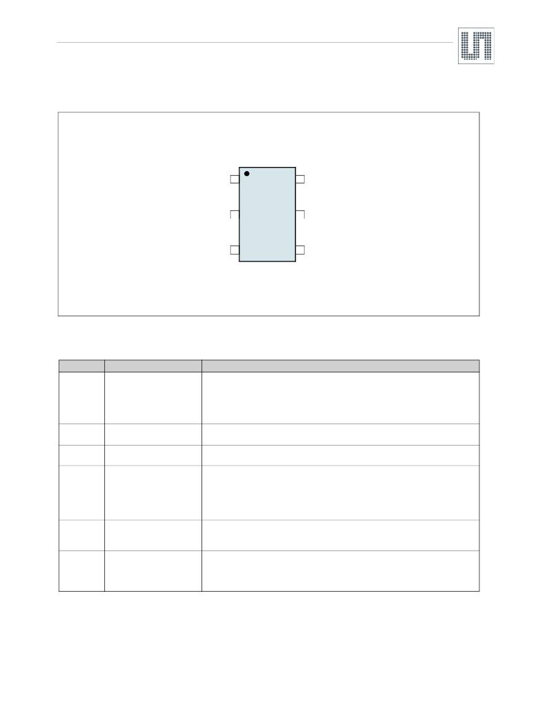
�4� Pin� Assignments�
�Figure� 2.� Pin� Assignments� (Top� View)�
�SW� 1�
�6� VIN�
�4.1� Pin� Descriptions�
�Table� 2.� Pin� Descriptions�
�GND� 2�
�FB� 3�
�AS1329�
�5� VOUT�
�4� SHDNN�
�Pin� Number�
�1�
�2�
�3�
�4�
�5�
�6�
�Pin� Name�
�SW�
�GND�
�FB�
�SHDNN�
�VOUT�
�VIN�
�Description�
�Switch� Pin� .� Connect� an� inductor� between� this� pin� and� V� IN� .� Keep� the� PCB� trace� lengths� as�
�short� and� wide� as� is� practical� to� reduce� EMI� and� voltage� overshoot.� If� the� inductor� current�
�falls� to� zero,� or� pin� SHDNN� is� low,� an� internal� 100� ?� anti-ringing� switch� is� connected� from� this�
�pin� to� V� IN� to� minimize� EMI.�
�Note:� An� optional� Schottky� diode� can� be� connected� between� this� pin� and� V� OUT� .�
�Signal� and� Power� Ground� .� Provide� a� short,� direct� PCB� path� between� this� pin� and� the�
�negative� side� of� the� output� capacitor(s).�
�Feedback� Pin� .� Feedback� input� to� the� g� m� error� amplifier.� Connect� a� resistor� divider� tap� to� this�
�pin.� The� output� voltage� can� be� adjusted� from� 2.5� to� 5V� by:� V� OUT� =� 1.23V[1� +� (R� 1� /R� 2� )]�
�Shutdown� Pin� .� Logic� controlled� shutdown� input.�
�1� =� Normal� operation,� 1.2MHz� typical� operating� frequency.�
�0� =� Shutdown;� quiescent� current� <1μA.� If� SHDNN� is� undefined,� pin� SW� may� ring.�
�Note:� In� a� typical� application,� SHDNN� should� be� connected� to� V� IN� through� a� 1M� ?� pull-up�
�resistor.�
�Output� Voltage� Sense� Input� and� Drain� of� the� Internal� PMOS� Synchronous� Rectifier� .�
�Bias� is� derived� from� V� OUT� when� V� OUT� exceeds� V� IN� .� PCB� trace� length� from� V� OUT� to� the�
�output� filter� capacitor(s)� should� be� as� short� and� wide� as� is� practical.�
�Input� Voltage� .� The� AS1329� gets� its� start-up� bias� from� V� IN� unless� V� OUT� exceeds� V� IN� ,� in�
�which� case� the� bias� is� derived� from� V� OUT� .� Thus,� once� started,� operation� is� completely�
�independent� from� V� IN� .� Operation� is� only� limited� by� the� output� power� level� and� the� internal�
�series� resistance� of� the� supply.�
�www.ams.com/DC-DC_Step-Up/AS1329�
�Revision� 1.12�
�2� -� 20�
�发布紧急采购,3分钟左右您将得到回复。
相关PDF资料
MC34063SMDBGEVB
BOARD EVALUATION MC34063
HCM06DRYN
CONN EDGECARD 12POS DIP .156 SLD
SJA7501-1-1/2-50-BLACK
LOOP BLACK 1 1/2" X 50YD X 0.12"
EBM11DRYH
CONN EDGECARD 22POS DIP .156 SLD
EEV-HB1C100R
CAP ALUM 10UF 16V 20% SMD
TARQ155K020
CAP TANT 1.5UF 20V 10% AXIAL
RE-243.3S/H
CONV DC/DC 1W 24VIN 3.3VOUT
L-07C4N3SV6T
CER INDUCTOR 4.3NH 0402
相关代理商/技术参数
AS1329ABTTT
制造商:AMS 功能描述:IC, STEP-UP DC/DC CONVERTER, 6-SOT-23; Primary Input Voltage:1.2V; No. of Outputs:1; Output Voltage:5V; Output Current:220mA; No. of Pins:6; Operating Temperature Min:-40C; Operating Temperature Max:85C; Output Current Max:315mA ;RoHS Compliant: Yes
AS1329A-BTTT
功能描述:IC REG BOOST SYNC ADJ TSOT23-6 RoHS:是 类别:集成电路 (IC) >> PMIC - 稳压器 - DC DC 开关稳压器 系列:- 标准包装:1,000 系列:- 类型:降压(降压) 输出类型:可调式 输出数:1 输出电压:0.6 V ~ 4.5 V 输入电压:3 V ~ 5.5 V PWM 型:电流模式 频率 - 开关:3MHz 电流 - 输出:1.5A 同步整流器:无 工作温度:-40°C ~ 125°C 安装类型:表面贴装 封装/外壳:6-WDFN 裸露焊盘 包装:带卷 (TR) 供应商设备封装:6-LLP-EP(3x3) 产品目录页面:1300 (CN2011-ZH PDF) 其它名称:LM2831ZSDLM2831ZSDTR
AS1329B
制造商:AMSCO 制造商全称:austriamicrosystems AG 功能描述:Low Voltage, Micropower, DC-DC Step-Up Converters
AS1329B EB
功能描述:BOARD EVAL AS1329B RoHS:否 类别:编程器,开发系统 >> 评估板 - DC/DC 与 AC/DC(离线)SMPS 系列:- 产品培训模块:Obsolescence Mitigation Program 标准包装:1 系列:True Shutdown™ 主要目的:DC/DC,步升 输出及类型:1,非隔离 功率 - 输出:- 输出电压:- 电流 - 输出:1A 输入电压:2.5 V ~ 5.5 V 稳压器拓扑结构:升压 频率 - 开关:3MHz 板类型:完全填充 已供物品:板 已用 IC / 零件:MAX8969
AS1329BBTTT
制造商:AMS 功能描述:IC STEP-UP DC/DC CONVERTER 6-SOT-23 制造商:AMS 功能描述:IC, STEP-UP DC/DC CONVERTER, 6-SOT-23; Primary Input Voltage:1.2V; No. of Outputs:1; Output Voltage:5V; Output Current:220mA; No. of Pins:6; Operating Temperature Min:-40C; Operating Temperature Max:85C; Output Current Max:315mA ;RoHS Compliant: Yes
AS1329B-BTTT
功能描述:IC REG BOOST SYNC ADJ TSOT23-6 RoHS:是 类别:集成电路 (IC) >> PMIC - 稳压器 - DC DC 开关稳压器 系列:- 标准包装:50 系列:- 类型:升压(升压) 输出类型:可调式 输出数:1 输出电压:5 V ~ 25 V 输入电压:2.3 V ~ 5.5 V PWM 型:电流模式 频率 - 开关:600kHz,1.2MHz 电流 - 输出:1A 同步整流器:无 工作温度:-40°C ~ 85°C 安装类型:表面贴装 封装/外壳:8-TSSOP,8-MSOP(0.118",3.00mm 宽) 包装:管件 供应商设备封装:8-MSOP
AS1329B-EB
制造商:ams 功能描述:AS1329B Evaluation Board
AS1329B-TT_EK_ST
功能描述:AS1329B - DC/DC, Step Up 1, Non-Isolated Outputs Evaluation Board 制造商:ams 系列:- 零件状态:有效 主要用途:DC/DC,步升 输出和类型:1,非隔离 功率 - 输出:- 电压 - 输出:3.3V 或 5V 电流 - 输出:570mA 电压 - 输入:0.85 V ~ 5 V 稳压器拓扑:升压 频率 - 开关:1.2MHz 板类型:完全填充 所含物品:板 使用的 IC/零件:AS1329B 标准包装:1